Table Of Content

Don Kaufman is our Business Development Manager and has been with Cirexx International since 2006. He has over 33 years of sales and technical experience in the printed circuit board industry, which provides intrinsic value to customers. Don has extensive knowledge regarding integrated circuits, materials, specialty laminates, chemicals and equipment.
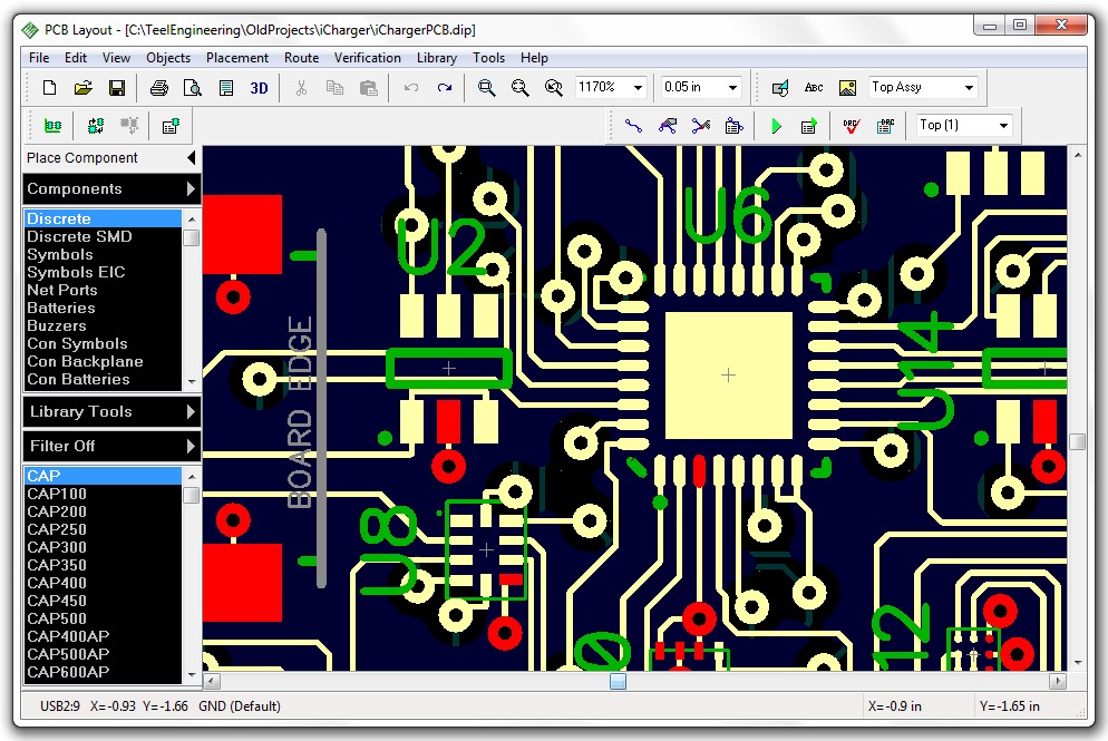
AUTOMATICALLY ROUTING THE BOARD
Plus, as it’s technically part of Fusion 360, you have seamless integration with a vast array of advanced CAD, CAM, and CAE tools, making it a great all-in-one solution for many electrical engineering applications. LibrePCB aims to deliver free, open source, and easy-to-use PCB design for everyone from students and hobbyists to experts and professional designers. There are no strings, restrictions, or caveats, you get full functionality at zero cost whatever your skill level or the project. If the browser version isn’t for you, there’s also a standalone version. EasyEDA is available in two tiers – a free version supported by ads and a paid professional/enterprise, that’s ad free and features improved collaboration tools and customer support. EasyEDA also features LCSC parts and JLCPCB PCB ordering, so you can turn your project into a physical PCB quickly and efficiently.
Power and Ground Planes
There’s also a quickstart template library with hundreds of boards to choose from, ideal for starting a project, especially in an educational context. And, should you want to bring your designs to life, there’s an integrated hassle-free manufacturing option for your custom-made PCBs, which are tested before delivery. KiCad features a schematic editor, suitable for everything from simple designs all the way to complex multi-sheet projects.
May the Flux (Copilot) Be with You! - EE Journal
May the Flux (Copilot) Be with You!.
Posted: Thu, 07 Sep 2023 07:00:00 GMT [source]
PLACING THE COMPONENTS ON THE SCHEMATIC DIAGRAM
The PCB design tutorial provided just a quick overview into the design process with Altium Designer. Check out other Getting Started guides for insight into using robust features like Draftsman® and ActiveRoute®. 11) Ensure the Launch main design rules dialog box is checked and click Finish. New users of Altium software may find value in reading the article Exploring Altium Designer for an explanation of the interface, information on how to use panels, and guidelines for managing design documents.
PCB design basics
5) The error will be highlighted in a zoomed view similar to the below image. Correct the trace Width in the Properties panel or by entering Ctrl-Z to undo your width change. Save the file, and assure there are no DRC errors by rechecking again. Press Ctrl-Z twice and see that the auto-routing and Un-Route All command can be reversed. If you click Finish before completing the entire Wizard, the newwidth rule will be created using the system defaults for the component type you selected.
Step 8: Gerber File Generation
To flip the orientation of the transistor that is floating on the cursor, press the X key on the keyboard. 5) Continue placement by clicking on the pause button that is displayed in the center of the schematic. Once the transistor is in the desired position, left mouse click or press Enter on the keyboard to place the transistor onto the schematic. 4) Before placing the part on the schematic, press the Tab key to open the properties panel and pause placement.
The location of components like power connections, potentiometers, LEDs, and audio jacks in your finished project will affect how your PCB is laid out. Or do you need to put a volume potentiometer next to a gain potentiometer? For the best user experience you might have to make some compromises and design the rest of your PCB around the locations of these components. You can always etch PCBs at home with a process that’s similar to developing prints from photographic film. It’s much easier (and cheaper) to get your PCB made by a professional manufacturer. To demonstrate the process, I’ll use an online service called EasyEDA to design a PCB layout for an LM386 audio amplifier, then I’ll have it manufactured and show you the results.
PCB Layout Basics Part 1: Getting Started with Circuit Board Design Software
You’ve reached the end of the design phase and it’s on to manufacturing. Next, your manufacturer will review the design to ensure it conforms to their processing capabilities. If everything passes a final DFM review, your board will go into production and assembly. PCB design has evolved from the early days of sticky back component patterns and tape placed on a mylar sheet that was then photographed to create a production tooling master artwork used for manufacturing. With the evolution in PCB design over the decades, the process, and individual roles of the key stakeholders of who does what, and when within the design process has evolved as well. Typically, PCB design falls under the Hardware (HW) design category of engineering.
One of the first steps is always creating a schematic, which refers to the design at the electrical level of the board’s purpose and function. Through-hole pads on copper pour could require the same thermal pad application as planes. When the pour is very large, it starts to look a lot like a plane, and so a thermal pad should naturally be applied if a through-hole pin will be soldered into that connection. A connection object cannot be edited with respect to properties in the usual manner; it cannot be selected in the design space, has no corresponding Properties panel mode or dialog and cannot be edited graphically.
There are also the likes of Eagle, which have limited free versions and unlimited paid versions. This allows you to download and use the software for free if you’re a student, and there are also plans for teachers and universities. Autodesk offers fantastic support and learning resources for Eagle, and it’s one of the most widely compatible CAD PCB software, being available on Mac, Windows, and Linux. Overall, it’s probably the most comprehensive and highest quality PCB design solution money can buy.
If necessary, you can create new circuit board design rules by following the steps of Altium Designer’s Design Rule Wizard. PCB design products include specialized tools that set them apart from hardware-focused CAD software. Separate editors for circuits, 2D schematics, and 3D models help engineers through the entire design lifecycle, from concept to assembly.
Sometimes the Snap To Object Hotspot feature pulls the cursor when it is not desirable, in this situation press the Ctrl key to temporarily inhibit this feature. 2) Check which layers are currently visible by looking at the Layer Tabs at the bottom of the workspace. If the Bottom Layer is not visible, press the L shortcut to open the Layers and Colors dialog, and enable the Bottom Layer by clicking the Eye Symbol next to the layer name.
For instance, surface mounted components are small and have a low profile, so you’ll be able to make the PCB smaller. Through hole components are larger, but they’re often easier to find and easier to solder. Supports high-frequency, high-speed, FPC, and high power PCB design. Easily replace components using the Device Manager, allowing for quick modification of component properties and standardized BOM output.
When we refer to a double sided or 2-layer board we are referring to the number of copper layers (2) in our lasagna. Printed circuit board is the most common name but may also be called "printed wiring boards" or "printed wiring cards". Before the advent of the PCB circuits were constructed through a laborious process of point-to-point wiring. This led to frequent failures at wire junctions and short circuits when wire insulation began to age and crack. KiCad's 3D Viewer allows easy inspection of your PCB to check mechanical fit and to preview your finished product.A built-in raytracer with customizable lighting can create realistic images to show off your work. The PCB editor will automatically insert a via (in accordance with the Routing Via design rule) as necessary when layersare changed.
OrCAD is an electrical design automation (EDA) CAD suite, now owned and supported by Cadence Design Systems. EasyEDA is an online PCB design tool, from Shenzhen Lichuang E-commerce Co.,Ltd headquartered in China. Xpedition Enterprise is a PCB design flow, providing integration from system design definition to manufacturing execution. Its technologies help to reduce design cycles by 50 percent or more while improving overall quality and resource efficiency. It’s important to note that the Printed Circuit Engineering Layout Professional is only one of the significant roles within the grand scheme of PCB design. The accepted recommended definition reads as follows and is shown pictorially.


No comments:
Post a Comment