Table Of Content
Through dynamic mechanical analysis, we find negligible catalyst loss, minimal changes in storage modulus and equivalent polymer backbone composition across multiple recycling cycles. This recycling process achieves 98% polymer recovery, 100% fibre recovery and 91% solvent recovery to create new vPCBs without performance degradation. Overall, this work paves the way for sustainability transitions in the electronics industry.
Library Management
Design rule checking ensures that things like trace width and the spacing between components falls within pre-defined parameters. Most EDA/ECAD programs have the ability to run design rule checks on your PCB layout. Altium Designer is a complete solution for PCB projects, from basic circuits to full avionics systems.
Component Placement
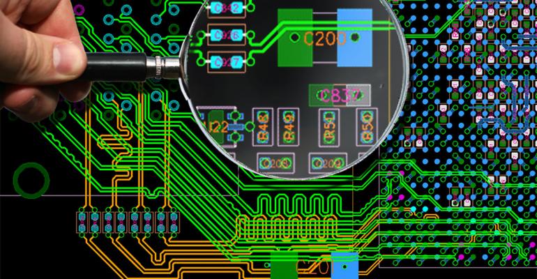
Before routing anything, try to get the layout to the point where all net crossings are minimized. To this day, I’m still surprised at the number of new designers that hesitate to place a ground plane in their PCB stackup. Many basic noise problems that affect digital and analog signals can be traced back to the absence of a ground plane in the device. In modern PCBs, it is a standard guideline to use a solid ground plane throughout your device. There are some exceptions where split planes or a star ground on a PCB are appropriate, but those approaches are not appropriate for the vast majority of digital and analog designs. This footprint has pad-to-pad spacing of about 9 mils, but it triggers a design rule error (seen in green) once the component is transferred to the PCB layout.
Explore recently added products
Once you’ve determined your device requirements for your application, Altium Designer allows you to encode these specifications in design rules. You can rest assured your layout will comply with your design rules, and you can check and correct any rules violations quickly and easily. These rule definition and checking features help you stay within standard design guidelines and help you build a device that meets your technical requirements.
MAKING CIRCUIT CONNECTIONS
To ensure a successful design, careful review of the layout is necessary, along with a thorough understanding of basic design rules and techniques outlined in the PCB design guide. In this article, TechSparks will provide essential pointers to enhance your PCB design process. After designing a schematic for a circuit, the next step is to design a PCB layout. PCB design is where you decide where the electronic components will fit on a PCB and where you draw the conductive traces to connect everything. At the end of the PCB design process, you can generate a set of Gerber files to send to a PCB manufacturer.
Understanding Simple DC Power Supply Circuits
Allegro X Design Platform, from Cadence Design System, offers engineers a system design platform that integrates logic/physical design, system analysis, and design data management for PCB and system design. But the following steps are more or less the same, no matter what software you use. It’s important to communicate with the PCB or flex application engineer during the beginning of any PCB design job and discuss everything you need or require for your project. Open and constant communication with your PCB provider ensures that you’re both on the same page, which can reduce the need for multiple extensive revisions. If you specify user-defined From Tos for only part of a net, the PCB Editor will set the remaining pin-to-pin connections (system-generated From Tos) to the Shortest topology. As such, a connection is not a design object that you can access or place.
The signals in your circuit should flow in a direct path from one section to another, which will keep the traces shorter. Use EasyEDA design to swiftly generate a free 3D structure of your PCB, streamline the structural design process, and export STEP files quickly. Allow multiple designers to collaborate effortlessly from any location or device, empowering teams to comment on designs and enhance teamwork effectiveness. All the PCB software we’ve reviewed generally offer the same core layout and schematic design features, but the quality varies a lot depending on the program. For example, the 3D renderings offered by professional solutions like Altium are considerably higher quality than those you get in free programs. There’s no denying that some software are better designed and easier to use than others, and it’s often the more professional paid solutions that are the most intuitive.

CircuitMaker – Best Free PCB Design Software for Beginners & Windows
Now is the time to add any labels, identifiers, markings, or reference designators to the layout. Reference designators are helpful in showing where specific components will go on the board. After you’ve placed the components and drill holes, you’re ready to route the traces, which means connecting segments of the path. Multiple extensive revisions can seriously delay the completion of your project — costing you time and money.
Before transitioning to the PCB layout, you must define the PCB shape and layer stack. If the PCB needs to fit inside an enclosure, the mechanical team dictates the PCB’s shape and mounting hole locations. Depending on the design’s density, these can vary from one to over 24. All files created by LibrePCB arehuman-readable, canonical and conceived very carefully.This allows to use version control systems on libraries and projects withoutstruggling with unintended or obfuscated diffs. When designing a multi-layer PCB, you may need to create links between the various layers of your PCB.
He is a member of IEEE Photonics Society, IEEE Electronics Packaging Society, American Physical Society, and the Printed Circuit Engineering Association (PCEA). Any design that you intend to produce as a physical product should be manufacturable at scale. ECAD software will allow you to implement any design feature you can imagine into your PCB layout.
Moreover, there are constraints and guidelines that must be followed to ensure your design can actually be manufactured. After you’ve arranged all of the components, it’s time to start drawing the traces. However, they won’t always show you the best way to route the traces, so it’s a good idea to refer back to your schematic to verify the correct connections. In our opinion, EasyEDA is a solid option for beginners and intermediate designers looking to power a range of projects thanks to a simple and intuitive UI.
For example, you can specify heavier copper or a different substrate based on your application. The layer stackup also determines the placement of the power and ground planes which can affect the electromagnetic compatibility (EMC) and signal integrity of the circuit. PCBs can have different layers depending on the complexity of the circuit design. A simple PCB may only have one or two layers, while more complex PCBs can have up to 16 or more layers. The layers of a PCB include the top and bottom layer, signal layers, power and ground planes, silkscreen, and solder mask.
At all stages of routing your design, the software monitors and manages the netlist connectivity. Because the PCB's Connectivity Analyzer automatically monitors the completion status of the net you are routing, you can route without regard to the arrangement of the pin-to-pin connections. Once you complete a connection, the entire net is reanalyzed and connection lines are added and re-optimized as necessary. Assembly and installation take less time when DFM principles are followed.
Renesas to Acquire PCB Design Software Leader Altium to Make Electronics Design Accessible to Broader Market and ... - Business Wire
Renesas to Acquire PCB Design Software Leader Altium to Make Electronics Design Accessible to Broader Market and ....
Posted: Wed, 14 Feb 2024 08:00:00 GMT [source]
This way you can keep the track lengths between components short and have better control of the return path. Using the right design software is important in PCB design, so be sure to check out our article on the The Top Five EDA/eCAD Programs for Circuit Design to find the best program for your needs. Altium Designer plus Altium 365 offers secure, version-controlled data management and real-time component information, reducing risks and enhancing manufacturability decisions. Intuitively manage an increasing number of nets and design objects to ensure design performance and requirements are met with a spreadsheet-like, object-based constraint editor. Bring together all aspects of your electronics design in one place to help you deliver better products faster than ever before.
One of the key concepts in electronics is the printed circuit board or PCB. It's so fundamental that people often forget to explain what a PCB is. This tutorial will breakdown what makes up a PCB and some of the common terms used in the PCB world. It’s easy enough to create schematic symbols and PCB footprints with Altium Designer, but everyone needs resources to stay inspired and overcome design challenges. Circuit board parts have been traditionally difficult to find, and many designers have spent hours creating these parts manually. Altium Designer offers access to a Manufacturer Part Search panel, which helps you quickly add components to your library.


No comments:
Post a Comment